
on WeChat to
follow us

Research
Follow

Address
92 Xidazhi Street, Nangang District, HarbinZipcode
150001Tel
0451-86413909,86402590 121
121 Recently, Prof. Jinzhong Wang’s Group successfully illuminated the advantages of plasma pre-treatment on two-dimensional (2D) bismuth telluride (Bi2Te3) large-area growth on Si-based substrates, providing a new strategy for improving compatibility of 2D materials on Si-based substrates. The related research was published in the journal of Advanced Functional Materials, entitled “Large-Area Bi2Te3 Flakes on Si-Based Substrates for Sensitive IR Imaging Photodetection at MWIR Optical Communication Wavelengths”.
Owing to the narrow bandgap and high mobility, Bi2Te3 could achieve photodetection at mid-wavelength infrared band, simultaneously integrating with Si-based substrates to utilize the mature process of complementary-metal-oxide-semiconductor (CMOS) system, which could greatly expand its application. Thus, it is very important to investigate how to synthesize 2D Bi2Te3 photodetector with satisfactory Si-based substrates integration. Si-based substrates compatibility is closely related to the surface state of the substrates. At present, most methods are difficult to completely clean the substrate surface and create conditions for the large-area growth of 2D materials, which makes it very difficult to directly grow large-area 2D materials on Si-based substrates. Furthermore, the area is related to the monolithic integration of the device, which is quite significant for its practical application.
To solve this problem, the group considered that plasma pretreatment could efficiently clean the residual pollutants on the substrate surface and create nucleation sites, providing favorable conditions for the large-area growth of 2D materials. Based on this, using chemical vapor deposition (CVD) method, the group successfully realized the large-area growth of Bi2Te3 flakes on the plasma pretreated Sio2/Si substrates, with a max-size of 0.16 mm.
The Bi2Te3 photodetector showed excellent infrared photodetection ability under the irradiation of 1550 nm light source, which was due to the high crystal quality and the in-situ preparation of the device. In addition, the detection performance of the device was significantly improved at lower temperature, and its specific detectivity (D*) significantly increased to 7.52×10¹² Jones at 82 K. This is mainly due to the low temperature suppressing the intrinsic excitation of 2D Bi2Te3 material, which greatly reduces the dark current of the device. As a typical narrow band gap material, Bi2Te3 is more significant of this phenomenon, leading to a sensitive and stable infrared detection of the detector. This research work provides a new idea for the large-area growth of 2D materials on Si-based substrate and an important basis for the unique advantages of 2D Bi2Te3 materials for infrared detection.
The first author of this paper is the Ph.D. candidate Yinze Zhang, School of Materials Science and Engineering. Researcher Dongbo Wang, assistant professor Wen He and Professor Jinzhong Wang are the co-corresponding authors of the paper, and Harbin Institute of technology is the first corresponding unit of this paper.
This work was financially supported by the National Key Research and Development Program of China (2019YFA0705201), the National Natural Science Foundation of China (U2032129, 62574067).
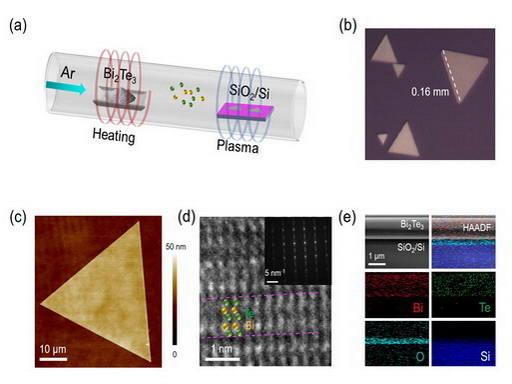
Figure 1. Characteristics on morphology and crystal structure of the Bi2Te3 flakes: a) Schematic illustration of CVD synthesis, b) Optical image, c) AFM image, d) HRTEM image, e) SEM image and EDS mappings.
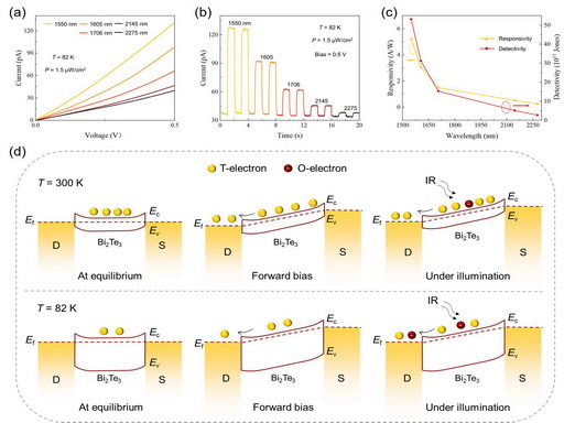
Figure 2. Performance of the Bi2Te3 photodetector, a) I-V curves, b) I-t curves, c) Responsivity and detectivity, d) Schematic band structures of the photodetector at 300 and 82 K.
Link of this paper:
https://advanced.onlinelibrary.wiley.com/doi/10.1002/adfm.202523704